Researchers from the Research Center Jülich (FZJ), the University of Stuttgart, the Leibniz Institute for High Performance Microelectronics (IHP) and their French partner CEA-Leti have achieved a breakthrough by developing the first electrically pumped continuous-wave semiconductor laser composed entirely of group IV elements, commonly known as the “silicon family”.
The growing adoption of Artificial Intelligence (AI) and the Internet of Things (IoT) is driving the need for more powerful and energy-efficient hardware solutions. Optical data transmission is the preferred choice for distances over one meter and increasingly favorable for shorter distances as it enables high-capacity data transmission with minimal energy loss. This trend highlights the possibility of incorporating cost-efficient Photonic Integrated Circuits (PICs) into future microchips, promising improved performance and reduced costs.
Recent progress has focused on monolithically integrating active optical components directly on silicon chips. Key components such as high-performance modulators, photodetectors, and waveguides have been successfully developed. However, creating efficient electrically pumped light sources made entirely from group IV semiconductors remains a major challenge.
Traditionally, light sources have relied on III-V materials, which are difficult and expensive to integrate with silicon. This new laser overcomes that barrier and is compatible with conventional CMOS technology, allowing seamless integration into established silicon manufacturing processes. This represents a transformative development that has the potential to fill the “last gap” in the silicon photonics ecosystem.
We have been exploring the fascinating potential of germanium-tin (GeSn) alloys for almost a decade. The development of efficient electrically pumped lasers has been one of our main goals from the beginning. This breakthrough is further evidence of the great potential of GeSn alloys in various applications, especially photonic applications.
Dr. Dan Buka, Group Leader, Research Centre Jülich
For the first time, researchers have demonstrated continuous-wave operation of an electrically pumped group IV laser on silicon.
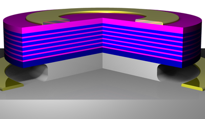
Unlike conventional germanium tin lasers that rely on high-energy optical pumping, this laser operates with low injection currents of just 5 milliamps (mA) at 2 volts (V), comparable to the power consumption of a light-emitting diode. The advanced multiple quantum well structure and ring geometry reduce power consumption and heat dissipation, allowing stable operation up to 90 Kelvin (K) or minus 183.15 degrees Celsius (°C).
Grown on standard silicon wafers used for silicon transistors, this laser will be the first truly “usable” group IV laser, although further optimization is required to lower the lasing threshold and achieve room temperature operation. The success so far of optically pumped germanium tin lasers, progressing from cryogenic to room temperature operation within a few years, suggests that the future looks promising.
Optically pumped lasers require an external light source to generate laser light, while electrically pumped lasers generate light by electrical current passing through a diode. Electrically pumped lasers are generally more energy efficient, converting electricity directly into laser light.
The research team led by Dr. Buka at the Jülich Research Centre PGI-9, in collaboration with partners such as IHP, the University of Stuttgart, CEA-Leti, C2N-Paris-Sud and Politecnico di Milano, has been pioneering the production of tin-based Group IV alloys for many years, bringing the vision of silicon photonics as a complete solution for next-generation microchips closer to reality.
Journal References:
Seidel, L. et al . (2024) Continuous-wave electrically pumped multiple quantum well lasers based on group IV semiconductors. Nature Communications . doi.org/10.1038/s41467-024-54873-z
sauce:
Jülich Research Center